During the made of a silicon solar cells single crystal wafers, polycrystalline wafers or thin films are using. Single crystal wafers are shred, (about 1/3 to 1/2 of a millimeter thick), from a large single crystal bullion which has been stretched out at around 1400 °C, which is a very expensive process. The silicon must be of a very high purity and have a near perfect crystal structure so it can be absorb the sunlight.
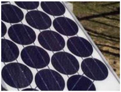
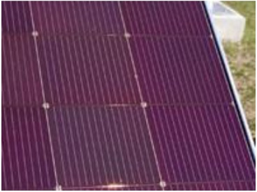
Crystalline silicon cells is directly related to solar system’s efficiency, therefore it dominates the photovoltaic market. However, single crystals are more effective because of expensive, cells are now often made from multi crystalline material rather than single in order to reduce
costs. According to, the modules have long lifetime (20 years and more) and their best
production efficiency is approaching 18% it can be said that crystalline silicon cell technology
is well established. Besides, amorphous silicon solar cells are cheaper but also less efficient
type of silicon cells. The silicon solar cells which are made form of amorphous thin films are
used to power a variety of consumer products. Larger amorphous silicon solar modules are
also becoming available with the improvement in the solar industry. a new
type of thin film modules are appearing on the market cadmium telluride and copper indium
dieseline which is also offer low cost with acceptable conversion efficiencies. High-efficiency
solar cells design from gallium arsenide, indium phosphide or their derivatives are used in
specialized applications such as to power satellites or in systems which operate under high-
intensity concentrated sunlight.
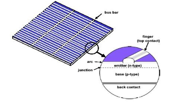
In Figure shows below the structure of a typical silicon solar cell. The electrical current
generated in the semiconductor is extracted by contacts to the front and back of the cell. As
can been seen at the top contact structure also called finger should be allow light to
pass through that supply current to a larger bus bar. Transparent conducting oxide is also
used on a number of thin film devices. When solar cell absorbing the sunlight meantime
it should be minimize the reflection of light in order to increase the efficiency. This is
called the antireflection coating ( ARC) which is covered with a thin layer of dielectric
material
The energy transformation in solar cells is different from the classical heat engine process, so the limitations and losses that occur in more detail. The fundamental mechanisms responsible for losses in solar cells are explicit from the discussion of solar cell operation. A considerable part of the solar spectrum is not utilized because of the inability of a semiconductor to absorb the below-band gap light which causes from the heat is produced on carrier generation in the semiconductor by photons with energy in excess of the band gap. Losses can be reduced, a device called tandem cell because going over to more complex structures based on several semiconductors with different band gaps. The top cell of tandem is made of a high band gap semiconductor, and converts the short wavelength radiation. The transmitted light is then converted by the bottom cell. This adjustment tenders considerably the achievable efficiency for the system. High efficiency space cells operating at close to 30% are available